Imagine a world in which lasers can draw entire circuit boards, where ceramic bowls normally used as pottery can produce electricity when exposed to light.
Layered materials promise this performance. Since 2004, when University of Manchester physicists isolated graphene – a one-atom-thick carbon sheet – the potential of these unusual nanoscale substances has intrigued scientists.
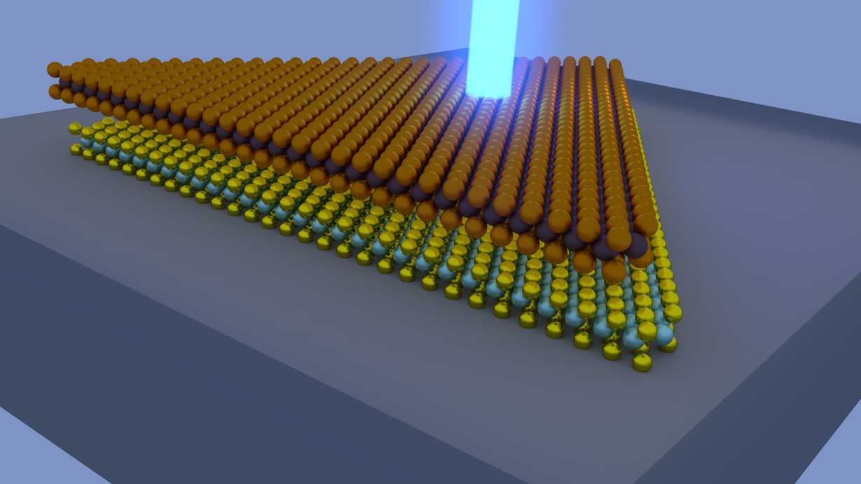
Layered materials, expected to dominate nanoscience in this century, have electronic, optical, magnetic and chemical properties that could make them useful in cellphone circuits or other small and flexible electronic devices. They can be made of a variety of compounds, each with different properties, in atomically thin layers stacked on top of one another. Sheets of metal could be placed on semiconducting or insulating layers, for instance. The different materials interact weakly, creating a route for electrons to flow freely, conducting electricity.
“The interactions between sheets are so weak that we can stack anything on top of anything,” says Aiichiro Nakano, a computational physicist at the University of Southern California. “Suddenly, there are infinite possibilities for designing new materials.”
Nakano’s vision is to develop layered materials that conduct electricity when exposed to light. To get there, however, he and his colleagues first must better understand how these materials interact with photons at a fundamental level. They’re attacking the problem with an allocation of supercomputing time from the Department of Energy INCITE (Innovative and Novel Computational Impact on Theory and Experiment) program. Their project also has been chosen for the Early Science Program on Aurora, the next major supercomputer to launch at the Argonne Leadership Computing Facility, a DOE Office of Science user facility at Argonne National Laboratory near Chicago. Early science projects will test the new machine before it enters full production. DOE expects to complete Aurora in 2021.
‘We were able to show that light is very efficient in moving atoms.’
Nakano is part of Materials Genome Innovations for Computational Software (MAGICS). Directed by USC’s Priya Vashishta, it’s one of three DOE-supported institutes the Obama administration established in its 2011 Materials Genome Initiative. It’s designed to accelerate the pace at which new materials are developed and brought to market, a process that ordinarily takes 20 to 30 years.
If Nakano succeeds in finding layered materials that become conductors when exposed to light, lasers could act like pens to draw an electronic circuit, accelerating and simplifying what’s now a time-intensive and laborious process. Using light to print circuits “would be much simpler, faster, and cheaper,” he says.
But to develop materials with changeable properties, Nakano and his colleagues must delve into their subatomic details. It’s a challenging task, given how many electrons there can be in a single sheet. Light striking atoms in the substance excite electrons, which start moving rapidly. Their respective phonons – heat particles that couple them to their atoms – help to move heavier atoms. This atomic rearrangement can transform semiconductors to conducting metals. “That’s the first breakthrough: We were able to show that light is very efficient in moving atoms.”
To evaluate how different materials respond to light, the researchers perform simulations on Mira, Argonne’s IBM Blue Gene/Q supercomputer. The research demands massive computer power because the scientists must understand the distribution of electrons at every possible stage and location.
The team uses modeling techniques such as non-adiabatic quantum molecular dynamics, which calculates the fast movements of light-excited electrons. This technique uses the initial positions of atoms observed via X-ray diffraction to predict what happens to them once light is introduced. Nakano and his colleagues want to perform a large number of non-adiabatic quantum molecular dynamic calculations involving 10,000 atoms to characterize how layered materials respond to light.
The quantum mechanics of these electrons is inherently complex, so Nakano and his colleagues designed simulation engines that use a technique called divide-conquer-recombine to take findings from smaller data sets and extrapolate them to approximations on larger data sets. “We’ll do 100 simulations, each containing just 100 atoms but talking to each other, and then we’ll assemble them to an approximation for the entire 10,000 atoms,” Nakano says. The divide-conquer-recombine method, he says, will calculate the actions of every atom and electron while holding computational costs low and increasing accuracy over brute-force computation, which is at least 10,000 times more time-consuming.
So far, Nakano and his colleagues have examined a layered material made with molybdenum diselenide, a compound useful for electronics, as a potential light-adaptable conductor. The researchers were able to show both experimentally and computationally that light could move molybdenum diselenide atoms, but it can’t turn it into metal. Nakano and his colleague, Rice University’s Pulickel Ajayan, are exploring other materials, such as alloys containing molybdenum, tungsten or rhenium in different proportions, that can become metal under light exposure.
Nakano also is working with Uwe Bergmann and David Fritz at Stanford University’s Linac Coherent Light Source to use ultrafast X-ray lasers to verify the simulations. “Experimenters used to think that theorists couldn’t reproduce their experiments, but now we have the technology to look at the same time and scale to compare” results from both perspectives, Nakano says. “For the first time, we can take movies of atoms moving at nanometer and picosecond scales. That’s really exciting.”
Nakano hopes these collaborations will yield useful materials that lead to new possibilities in electronics.